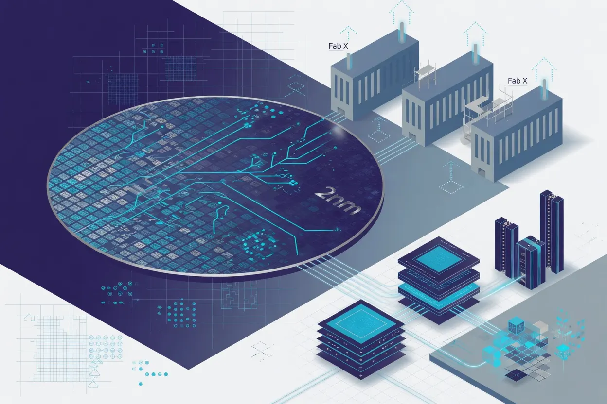
TSMC is scaling 2nm production and advanced packaging at the same time, treating both as equal constraints on how fast AI accelerators can reach customers.
The company is ramping its N2 process across multiple fabs simultaneously rather than proving the node at a single site before replicating it. TSMC is also expanding CoWoS and SoIC capacity, the packaging techniques that stack high-bandwidth memory on top of processors in AI chips. AI-driven process optimization is being built into the ramp to push yields and throughput as the build-out accelerates.
CoWoS capacity has been a genuine choke point in the AI chip supply chain, separate from how many wafers TSMC could produce. Running the packaging expansion in lockstep with the node ramp, rather than sequencing them, suggests TSMC has internalized a simple lesson: a finished 2nm wafer waiting on packaging ships the same number of chips as a wafer that was never made.
The "largest manufacturing expansion in semiconductor history" framing is worth some skepticism; that description gets applied at every major fab cycle. The genuinely unusual detail is the multi-fab simultaneous N2 ramp: foundries typically prove a node at one location before scaling out, and TSMC is departing from that cautious playbook, presumably because demand pressure has made the yield risk cheaper than the wait.